How AI Is Transforming Hiring Demand in Silicon Photonics
11 Nov, 202510 minutes
AI and photonics jobs are growing fast because classic electronic hardware is struggling to keep up with AI workloads, especially on power and data movement. Silicon photonics, co packaged optics, and optical neural networks are moving from research into real AI infrastructure, which creates fresh demand for very specific skills. Acceler8 Talent helps hiring managers understand where AI meets photonics, so you can plan design, manufacturing, and systems hires in a realistic way, not in a rush.
Key Takeaways:
- AI and photonics jobs are rising because AI workloads push the limits of copper based interconnects on power, bandwidth, and latency.
- Demand is strongest around optical interconnects, co packaged optics, and early photonic accelerators that support neural networks.
- Photonics engineers now contribute to AI chips and data center systems, not only telecom links or classic optics.
- Manufacturing, yield, and cost challenges in silicon photonics have a direct impact on the kind of process and test engineers you need.
- Photonic computing and optical neural networks are high risk, high reward research areas that need rare, often PhD level talent.
Why AI and photonics jobs are on the rise
Trying to figure out why AI and photonics roles have suddenly appeared in your headcount plan can be a real headache. One minute you are talking about GPUs and clusters, the next you are asked to hire someone who understands grating couplers and neural networks in the same conversation.
The simple story is this.
- AI models are bigger, and training runs are heavier than ever.
- Data centers face power and cooling pressure from AI clusters.
- Photonics promises faster data movement with lower energy use.
Once those three points line up, silicon photonics stops being a side project and becomes part of your core AI hardware roadmap. That is when the hiring pressure starts.
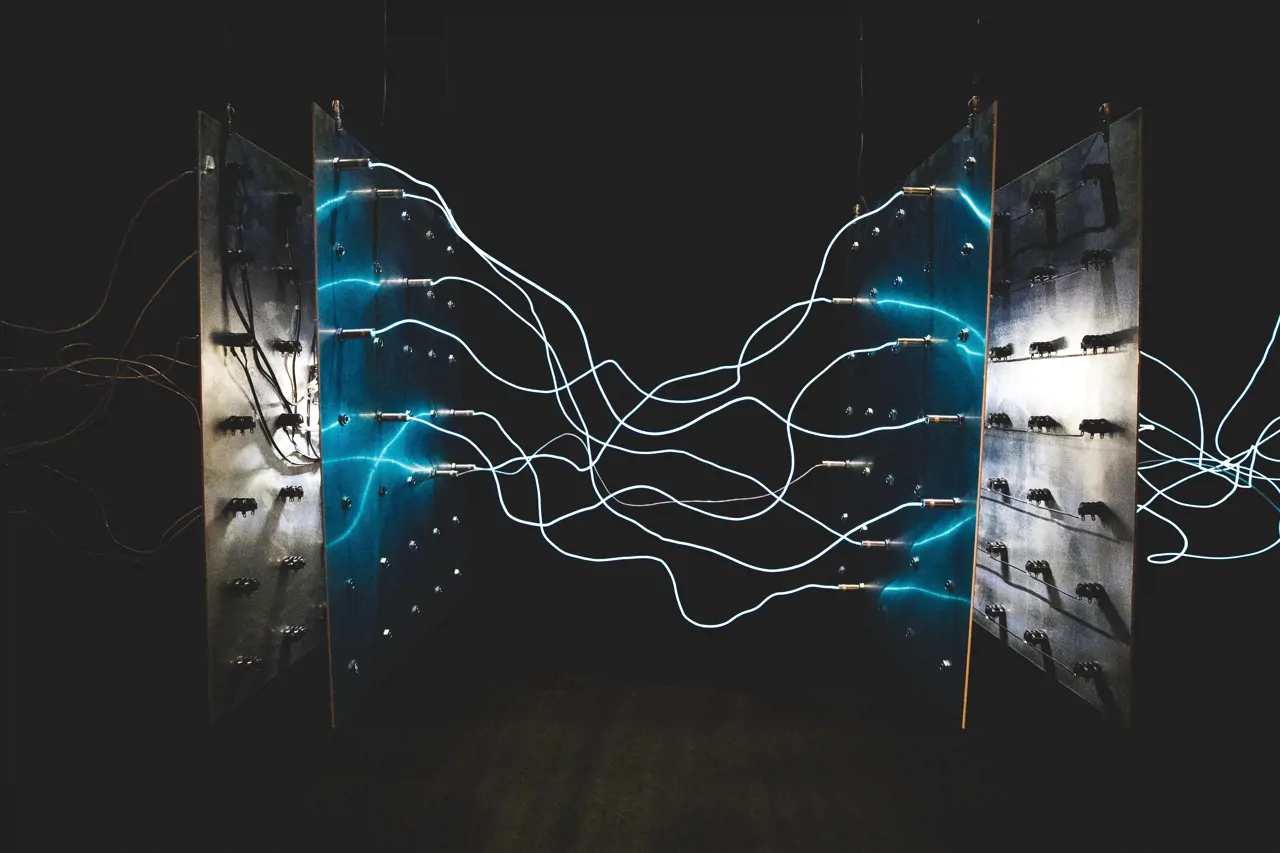
Where AI is driving silicon photonics growth
How is AI driving photonics growth?
AI is driving photonics growth by forcing vendors to replace or support copper based links with optical connections in AI servers and switches. The higher the AI traffic, the more you feel the limits of electrical signalling across boards and racks.
That shift shows up in growth plans for:
- Silicon photonic transceivers for short reach links inside data centers.
- Co packaged optics that sit very close to switch or compute silicon.
- Early optical accelerators that support AI workloads.
For you as a hiring manager, this means demand is not just for “photonics people” in general, but for engineers who know how optical parts behave inside AI servers and network gear.
Are photonics engineers working on AI chips?
Photonics engineers are very much working on AI chips, especially around the interfaces between compute die and optical components. Many new projects bring together digital design, packaging, and silicon photonics in the same stack.
Typical AI linked photonics roles include:
- Photonic integrated circuit designers who build modulators, filters, and couplers used in AI systems.
- Packaging engineers who handle co packaged optics for switches and accelerators.
- Test and reliability engineers who qualify photonic parts under realistic AI data center conditions.
A common mistake we see is assuming any photonics profile will fit. In practice, you often need people who understand process corners, thermal limits, and AI style traffic patterns, not just ideal optical behaviour.
Manufacturing, yield, and the reality of scaling silicon photonics talent
It is easy to focus on clever designs and forget that silicon photonics lives or dies on manufacturing yield and long term reliability. That has a huge impact on the jobs you need to fill.
Some of the pressures you will hear from your engineering leaders include:
- Variability across wafers when you integrate lasers, modulators, and detectors with CMOS logic.
- New failure modes compared with pure electronic chips, especially around temperature and ageing.
- High initial cost of new process flows, test equipment, and packaging lines.
Those realities mean you will see demand for:
- Process engineers who understand both CMOS and photonic device behaviour.
- Yield engineers who can link optical performance back to design and process steps.
- Reliability engineers who can build strong lifetime models for AI data center duty cycles.
Here is a quick insider tip. If your roadmap depends on volume deployment of silicon photonics, hiring only design profiles is risky. You also need people who can close the loop between design, fab, test, and field behaviour.
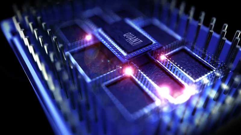
Photonic computing versus proven optical links
What skills overlap between AI and photonics?
The skills that overlap between AI and photonics sit around maths, modelling, and systems thinking. Both fields care about linear algebra, signal processing, and how small changes ripple through complex systems.
In practice, the strongest AI and photonics candidates often show:
- Working knowledge of neural networks or training pipelines.
- Solid understanding of optical devices and waveguide behaviour.
- Experience using simulation tools for both photonics and circuits or algorithms.
That said, there is a big difference between engineers who support optical interconnects, and researchers who push true photonic computing or optical neural networks.
Photonic computing is still a high risk, high reward area. Many projects explore optical neural networks that run matrix operations in the optical domain but face real hurdles around non linearity, control, and thermal drift. Roles here usually call for PhD level physics or electrical engineering, plus a genuine research track record.
By contrast, work on optical interconnects and co packaged optics is much closer to commercial deployment. Those teams still want strong academic grounding, but they focus more on product timelines, yield, and standards.
You will also see other technologies in the mix, such as advanced electrical signalling and faster SERDES. Your leaders are likely weighing these against photonic options, which shapes how urgent and how large the photonics hiring wave will be.
How to plan AI and photonics hiring demand
The outcome you want is a realistic hiring roadmap that covers design, manufacturing, and systems, without underestimating how rare some profiles are.
Map your AI hardware roadmap - List AI chips, accelerators, and data center projects, and mark where silicon photonics, co packaged optics, or photonic computing appear.
Separate near term and long term work - Distinguish between optical interconnect projects that aim at near term deployment and high risk photonic computing research, because the talent profiles and timelines are very different.
Group roles by design, manufacturing, and systems - Create role families for PIC design, packaging, test, yield, and system architecture, so you do not write one vague “photonics engineer” description for everything.
Define AI depth per role - Decide whether each role needs basic awareness of AI workloads, hands on experience with neural networks, or true AI research depth. Capture that clearly in briefs.
Account for manufacturing and cost pressures - Work with your hardware leaders to understand where yield, reliability, and cost are most sensitive, and prioritise process and reliability hires in those areas.
Plan for rare research profiles - For photonic computing or optical neural network work, expect smaller pools and longer search times, and consider links to universities and research labs.
Use internal growth where possible - dentify strong optics, process, or test engineers who can gain more AI context, and give them a path into AI linked photonics roles. That reduces pressure on external hiring.
Revisit your plan with each tape out or deployment - Review your AI and photonics hiring needs at each major hardware milestone, because manufacturing data and field results will change your priorities.
FAQs on AI and photonics jobs and skills
Q: How is AI driving photonics growth in real hiring markets?
A: AI is driving photonics growth in real hiring markets by forcing data centers and chip makers to adopt optical links and silicon photonics, which then creates new roles in design, packaging, test, and systems engineering.
Q: Are photonics engineers working on AI chips as a main focus now?
A: Photonics engineers are increasingly working on AI chips as a main focus, especially on integrated optics, co packaged optics, and the interfaces between compute die and optical components.
Q: What skills overlap between AI and photonics in modern roles?
A: The skills that overlap between AI and photonics in modern roles include neural network understanding, strong maths, optical device knowledge, and the ability to model complex systems end to end.
Q: How do photonic computing and optical neural networks affect hiring plans?
A: Photonic computing and optical neural networks affect hiring plans by adding a small number of research heavy roles that need deep physics and AI expertise, often at PhD level, alongside more product focused photonics hires.
Q: How do competing technologies change the urgency for AI and photonics hiring?
A: Competing technologies like advanced electrical signalling and evolving co packaged optics roadmaps change hiring urgency because they influence how quickly your organisation will commit to large scale silicon photonics deployment.
About the Author
This article was written by a senior recruitment consultant who specialises in AI hardware, silicon photonics, and data center engineering. They work closely with hiring managers, chip architects, and photonics leaders across start ups and global companies, helping them plan realistic AI and photonics hiring strategies and secure scarce talent in competitive markets.
Shape your AI and photonics hiring strategy with Acceler8 Talent
If you need to fill AI and photonics jobs across silicon photonics, AI chips, photonic computing, optical neural networks, hardware AI integration, and machine learning hardware, Acceler8 Talent can help you build the right team.
Contact Acceler8 Talent today to start building a focused AI and photonics hiring plan, secure specialist silicon photonics, AI chip, and ML hardware engineers, and close critical gaps in your AI infrastructure talent pipeline.